AI training, inference and high-performance computing are driving switch capacity toward the 51.2 Tbps and 102.4 Tbps class. At the same time, 800G and 1.6T interfaces are increasing the number of high-speed optical links deployed inside data centers. The challenge is no longer bandwidth alone. Electrical signal loss, module power, cooling, front-panel density and maintenance are becoming system-level design constraints.
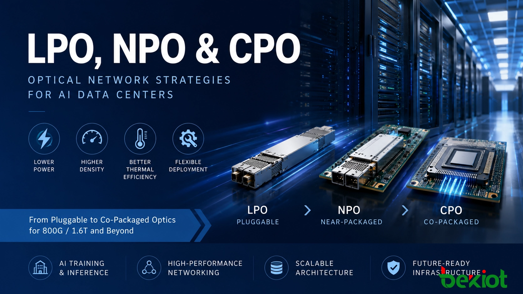
Traditional pluggable optics rely on relatively long PCB electrical paths between switching silicon and front-panel modules. Digital signal processors compensate for the resulting signal degradation, but that compensation adds power and heat. Linear-drive Pluggable Optics (LPO), Near-Packaged Optics (NPO) and Co-Packaged Optics (CPO) address the problem by changing where optical conversion takes place and progressively shortening the high-speed electrical path.
These architectures should not be viewed as a simple sequence in which one technology immediately replaces another. LPO emphasizes compatibility and lower power, NPO moves optical engines close to switching silicon while retaining a degree of replaceability, and CPO targets the highest integration and bandwidth density. Their value depends on the network being built.
Why Conventional Pluggable Optics Are Reaching Limits
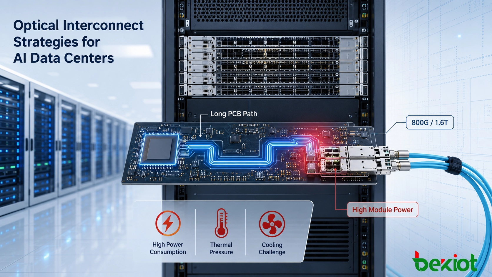
In a conventional architecture, switching silicon is mounted on the system PCB while optical modules are installed at the front panel. High-speed electrical signals may therefore travel tens of centimeters across the board before reaching the optical module.
At 112G and 224G electrical signaling rates, these traces become increasingly difficult to manage. Longer paths introduce insertion loss, crosstalk and waveform distortion. A module-side DSP is typically used to equalize and correct the signal before optical transmission, helping maintain reliable communication over the electrical channel.
The DSP solves an important signal-integrity problem, but it also contributes to three broader system constraints.
Optical power becomes a system-level issue
In high-density 800G and 1.6T deployments, optical-interface power is no longer a small fraction of switch consumption. A traditional 800G DR8 pluggable module can consume approximately 18–25 W per port, while optical modules may account for close to 50% of total equipment power in a dense configuration.
For a 64-port 800G switch, populating every port with modules in this range results in approximately 1,152–1,600 W of optical-module power alone. That load has direct consequences for power supplies, fan speed, airflow planning and rack-level cooling capacity.
Long electrical channels become harder to compensate
DSP-based equalization can correct many impairments, but it does not physically shorten the PCB connection. As interface rates rise, electrical loss and crosstalk become harder to control, and additional signal processing may add power and latency while the underlying channel remains long.
Front-panel density reaches physical limits
Traditional pluggable modules occupy cages on the equipment faceplate. As port counts increase, front-panel area becomes another limiting resource. Concentrating many high-power modules in the same area also creates a demanding thermal environment.
Three Ways to Shorten the Electrical Path
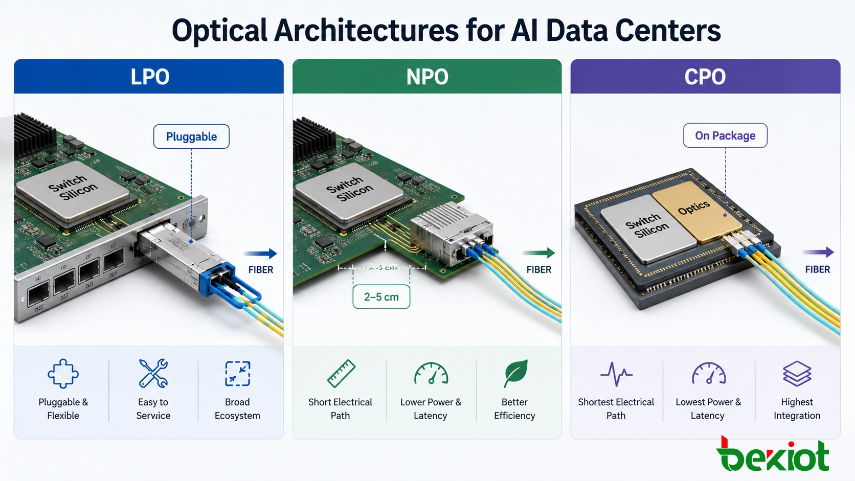
The essential difference among the three architectures is the distance between switching silicon and optical conversion. Moving optics progressively closer to the switching device reduces the electrical channel that must carry very-high-speed signals.
Linear-drive pluggable architecture
LPO preserves the familiar front-panel pluggable format but removes the DSP from the optical module. Linear signal-processing functions are shifted toward the switching side, while the module focuses mainly on optical conversion and linear amplification.
A simplified signal path is:
Switching Silicon → Linear Drive → Pluggable Optical Conversion → Fiber
The key advantage is operational continuity. The optical interface remains pluggable and can continue using established high-density form factors. Data-center operators can therefore reduce optical power without immediately changing the entire equipment maintenance model.
Near-package optical engines
NPO takes a more integrated approach. Instead of keeping the optical conversion function at the front panel, the optical engine is mounted on the system board near the switching silicon.
The electrical signal path can be shortened to approximately 2–5 cm:
Switching Silicon → 2–5 cm PCB Connection → Board-Mounted Optical Engine → Fiber
The architecture described in the technical material targets electrical signal loss below 13 dB and continues to avoid module-side DSP processing. An external laser source provides the optical source, while the nearby optical engine performs transmit and receive conversion.
Because the optical engine remains a separate component, NPO maintains a higher degree of serviceability than a fully co-packaged design while achieving greater integration than LPO.
Chip-level optical integration
CPO moves the optical engine onto the same package substrate as the switching silicon. Instead of centimeters of PCB routing, the high-speed electrical connection is reduced to the millimeter scale.
The path becomes:
Switching Silicon → Co-Packaged Optical Engine → Fiber
This approach removes most of the long electrical interconnect between the switching device and optical conversion stage. It therefore offers the strongest potential for high bandwidth density, low power and low electrical-path loss.
The trade-off is tighter coupling between optics and the switching platform. Service procedures, thermal design and reliability planning must be considered at system and package level rather than treating every optical interface as an independent front-panel module.
Comparing Power, Density and Serviceability
There is no single optical architecture that is optimal for every data center. Lower power and shorter electrical paths must be balanced against maintenance, platform complexity, deployment flexibility and technology maturity.
| Design Factor | DSP Pluggable | LPO | NPO | CPO |
|---|---|---|---|---|
| Power Consumption | High | Lower | Lower | Lowest |
| Bandwidth Density | Lower | Moderate | High | Highest |
| Integration Level | Low | Low to Moderate | High | Highest |
| Field Serviceability | Excellent | Good | Moderate | More Complex |
| Deployment Flexibility | Very High | High | Moderate | Lower |
| Typical Role | Mature general-purpose optics | Power-efficient migration | Higher-density new systems | Ultra-dense future platforms |
LPO changes the module electronics while preserving the physical operating model of a conventional pluggable interface. This makes it comparatively straightforward to introduce into environments where field replacement remains important.
NPO accepts more system integration in exchange for a much shorter electrical path. Because the optical engine remains separate from the switching package, it offers a compromise between electrical efficiency and maintainability.
CPO places maximum emphasis on integration. Its value becomes stronger as bandwidth density rises and the electrical link itself becomes a dominant limitation. The same integration, however, means maintenance cannot be planned in exactly the same way as with front-panel optics.
Where Each Architecture Fits Best
The most effective deployment strategy starts with the data-center scenario rather than selecting the most integrated technology by default.
Existing facilities and AI inference clusters
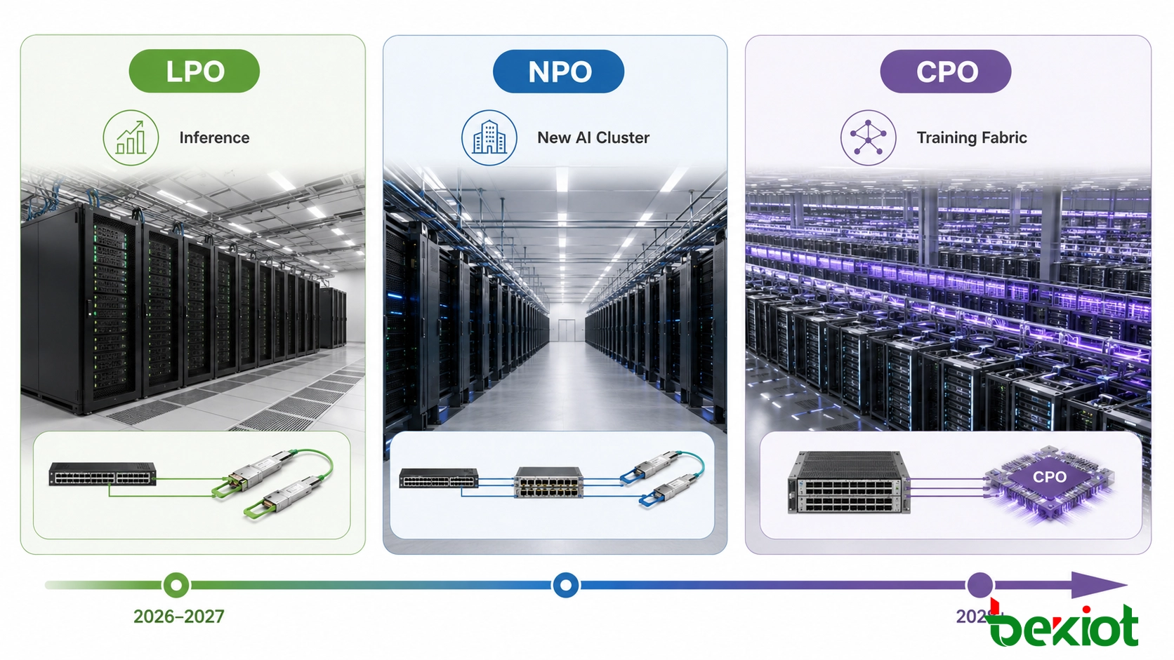
LPO is well suited to brownfield data-center upgrades where power reduction is required but operators still want a familiar pluggable interface. The technical roadmap positions it for 800G and 1.6T short- and medium-distance transmission, including AI inference clusters and existing facilities with limited cooling headroom.
This type of deployment can reduce the power burden associated with module-side DSP processing without requiring an immediate move to board-mounted or package-integrated optics.
New medium-scale computing sites
NPO is better aligned with new equipment designs where PCB layout can be optimized around short electrical channels. It is intended for 800G and 1.6T rack-level or short-distance interconnection while balancing higher integration with practical maintenance requirements.
For a greenfield AI data center, this architecture allows system designers to shorten the electrical path at the hardware-design stage instead of continuously compensating for a long front-panel connection.
Very large training fabrics
CPO is positioned for very large AI and high-performance computing clusters where bandwidth density and energy efficiency become more important than conventional optical-module replacement procedures.
At 1.6T and beyond, reducing the electrical path to the package level becomes increasingly attractive. The architecture is especially relevant to ultra-short-distance, high-radix switching systems in large training fabrics, where thousands of accelerators generate enormous east-west traffic.
Planning a Staged Migration
An optical-network upgrade should be designed around power budgets, switch lifecycle, service procedures and expected interface speed. Deploying the most integrated architecture everywhere may create unnecessary cost and maintenance complexity.
For an operating data center, a staged path can begin by identifying switches where optical modules consume a large share of equipment power. If the platform still requires front-panel serviceability, a lower-power pluggable approach may offer the most practical first step.
New switch designs provide greater freedom. Moving the optical engine onto the PCB and positioning it within a few centimeters of the switching silicon can reduce electrical-channel loss before it becomes severe enough to require extensive compensation.
Fully co-packaged optics becomes more compelling when interface speeds, switch radix and thermal density make conventional front-panel electrical paths increasingly difficult to sustain.
A practical decision framework can therefore be summarized as follows:
Use a pluggable linear-drive approach when lower power and field replacement are both important.
Move optics near the package when a new platform can support board-level optical engines and shorter PCB paths.
Consider co-packaged integration when maximum bandwidth density and minimum electrical-path length become primary design constraints.
Hybrid deployment is also reasonable. Different switch tiers, equipment generations and cluster sizes can use different optical architectures within the same data-center environment.
Market Direction Through 2028
The technology roadmap indicates a gradual transition rather than a single replacement event.
LPO began moving into larger-volume adoption from 2025. During 2026, 800G and 1.6T implementations are positioned for batch deployment in AI inference and existing data-center upgrade scenarios. The market outlook cited in the technical material estimates total LPO shipments of approximately 3–4 million units in 2026.
NPO follows a later adoption curve. The source places 1.6T NPO in a stage of technical maturity during 2026, with small-volume shipment expected in the second half of 2026 and larger-scale deployment beginning in 2027.
CPO has the longest integration cycle. The roadmap expects initial 1.6T pilot shipments around the end of 2026, followed by broader commercial deployment during 2027–2028. For next-generation 3.2T CPO, wider implementation is expected to develop after 2028.
The resulting deployment pattern is complementary. During 2026–2027, LPO and NPO are expected to address a large share of the 800G and 1.6T short- and medium-distance market, particularly existing data-center upgrades and new medium-scale AI clusters. Beyond 2028, CPO becomes more relevant to 3.2T and higher-speed ultra-large-scale training fabrics.
This does not mean that one architecture disappears when another scales. Different levels of integration solve different operational problems, so multiple approaches can remain active across data-center generations.
Final Notes
The shift from traditional pluggable modules toward LPO, NPO and CPO is fundamentally a response to an electrical interconnect problem created by rapidly increasing optical bandwidth.
At 51.2 Tbps and 102.4 Tbps switch capacities, a design based on long PCB traces, DSP compensation and large numbers of high-power front-panel modules places increasing pressure on power delivery, cooling and physical density. Shortening the electrical path changes that balance.
LPO offers the least disruptive path by retaining a pluggable interface while simplifying module-side signal processing. NPO brings the optical engine to within a few centimeters of the switching silicon, improving electrical efficiency while retaining some replaceability. CPO brings optics onto the same package substrate, targeting the highest bandwidth density and lowest electrical-path loss.
The appropriate solution therefore depends on where the network is in its lifecycle. Existing data centers may prioritize compatibility and maintainability, new AI sites can optimize board-level integration, and future ultra-dense training systems may require package-level optical integration. Treating these architectures as complementary options rather than universal replacements provides a more practical path toward 800G, 1.6T and future 3.2T networking.
FAQ
Can LPO still use standard pluggable optical form factors?
Yes. The architecture described in the technical material retains standard pluggable formats such as QSFP-DD and OSFP. The major change is the removal of module-side DSP processing rather than the elimination of the pluggable physical interface.
Does NPO require the optical engine to be permanently attached to the switch package?
No. In the described NPO architecture, the optical engine is mounted near the switching silicon on the system board and can remain independently replaceable. This is one of the main differences between near-package and fully co-packaged integration.
What role does an external laser source play in near-package optics?
The NPO implementation described here uses an independent External Laser Source, or ELS, to provide optical power while the board-mounted optical engine handles optical transmission and reception.
Why does removing the module DSP require more attention to host design?
When module-side signal processing is reduced or removed, electrical-channel quality becomes more dependent on switching-silicon capabilities, PCB layout and the overall host implementation. Lower module complexity therefore places greater importance on system-level signal-integrity engineering.